Board Server Hardware
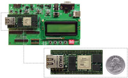
The board server hardware is hosted by a Xilinx FX12 FPGA, which contains a PowerPC 405 CPU. The FX12 mini module that we are using (left) is sold by Avnet: here is the product page. It is a tiny circuit board comprising a Xilinx Virtex-4 FPGA, SDRAM, Flash and an Ethernet header. The board is capable of running a full Linux 2.6 system on the PowerPC CPU within the FPGA, which is documented elsewhere.
The bit file for this FPGA is currently built using Xilinx ISE/EDK 10.1 service pack 3. Based on past experience, it is quite likely that future versions of ISE/EDK will not be able to generate the hardware correctly due to incompatibilities introduced by upgrades. For this reason, you should maintain a "frozen" ISE/EDK 10.1 installation that will never be upgraded.
The hardware consists mostly of IP cores provided by Xilinx and is generated entirely by EDK. It was originally based on an Avnet reference design for FX12. There are two custom IP cores. Here is the memory map:
| Device type | Instance name | Base address | High address | Note |
|---|---|---|---|---|
| RAM | DDR_SDRAM_32Mx16 | 0x00000000 | 0x03ffffff | |
| GPIO | BaseBoard_LEDs_3Bit | 0x81400000 | 0x8140ffff | Note |
| Int Cntlr | xps_intc_0 | 0x81800000 | 0x8180ffff | |
| MAC | TriMode_MAC_GMII | 0x81c00000 | 0x81c0ffff | Note |
| UARTLite | RS232 | 0x84000000 | 0x8400ffff | Note |
| Custom | tp0 (UART 0) | 0x8f000000 | 0x8f00ffff | Note |
| Custom | tp1 (UART 1) | 0x8f010000 | 0x8f01ffff | |
| Custom | tp2 (UART 2) | 0x8f020000 | 0x8f02ffff | |
| Custom | tp3 (UART 3) | 0x8f030000 | 0x8f03ffff | |
| GPIO | JTAG_Host_In | 0x8f100000 | 0x8f10ffff | Note |
| GPIO | JTAG_Host_Out | 0x8f110000 | 0x8f11ffff | |
| GPIO | Relay_Out | 0x8f120000 | 0x8f12ffff | |
| Custom | consoleswitch_0 | 0x8f200000 | 0x8f20ffff | Note |
| Flash | FLASH_2Mx16 | 0xff800000 | 0xffbfffff | Note |
| Block RAM | xps_bram_if_cntlr_1 | 0xfffff000 | 0xffffffff | Note |
Using EDK
To rebuild the FX12 bit file within EDK, obtain the file fx12-linux-hardware.zip from the download page and unpack it in a suitable location. Open the system.xmp project file using EDK. Then follow this procedure:
- Select: Project -> Clean All Generated Files.
- Select: Software -> Software Platform Settings.
Ensure that "OS" is standalone. Do not select any of the
libraries (xilmfs, xilflash, etc.). Click "OS and Libraries"
and ensure that stdout and stdin are both set to RS232.
Click Ok.
This step seems counter intuitive, because the intention is to run Linux on the platform. However, the first program that runs will be the boot loader, which is "standalone" and built into FPGA block RAM.
- Select: Hardware -> Clean Netlist.
This step has the side effect of generating the Makefile.
- Launch an EDK Shell (using the Start Menu group for EDK
on Windows, or by sourcing the EDK settings.sh file on
Linux). Move to the project directory and run:
This step is also counter intuitive, because the same operation is supposed to be provided by Update Bitstream in the Device Configuration menu. However, ISE/EDK 10.1 has some bugs that make some menu options unreliable. These bugs tend to mask real errors with GUI exceptions. Therefore, it is best to build the project at the command line.make -f system.make init_bram - When the process completes, use project dir/implementation/download.bit as the bit file.
If you add new devices or change the memory map, you have to make a new version of the Linux kernel. For this, you need to generate a new "fdt.dts" file in EDK. The procedure is as follows:
- Ensure that you have installed "gen-mhs-devtree" in EDK. This is included in fx12-linux-software.zip from the download page.
- Select: Software -> Software Platform Settings. Change "OS" to fdt. Click Ok.
- On the "OS and Libraries" page, change "bootargs" to read "console=ttyUL0 root=/dev/ram0 init=/sbin/init rw".
- Select: Software -> Generate Libraries and BSPs.
- When the process completes, search for fdt.dts in the project directory, and copy it to the Linux kernel directory linux-2.6-xlnx/arch/powerpc/boot/dts. You will need this in order to build the Linux kernel.
- Consider restoring the standalone OS settings (see above) to avoid the risk of building a bit file without a working boot loader.
Baseboard LEDs
The three baseboard LEDs are used to report the status of the system. The codes vary depending on the baseboard being used:
| LED State | Meaning | |||||||
|---|---|---|---|---|---|---|---|---|
| Avnet FX12 Prototyping Baseboard | In-House Virtex 4 Motherboard | |||||||
| DS1 | DS2 | DS3 | J261 | J263 | J264 | |||
| off | off | off | on | on | on | Undefined | ||
| off | off | on | on | off | on | Boot loader running (waiting 10 seconds before starting kernel) OR Embedded board server software starting | ||
| off | on | off | on | on | off | Boot loader expecting Intel Hex records OR Embedded board server software has exited abnormally | ||
| off | on | on | on | off | off | Linux kernel is booting | ||
| on | off | off | off | on | on | User space has been reached - init scripts are running | ||
| on | off | on | off | off | on | User space was reached, but either the network update failed, or the Flash memory was not initialised with configuration data | ||
| on | on | off | off | on | off | Embedded software is doing something | ||
| on | on | on | off | off | off | Embedded software is waiting for a command | ||
MAC
The FX12 FPGA includes two Ethernet MACs which can operate at 10MB/s, 100MB/s and 1000MB/s speeds. (Note: the software driver has only been tested at 100MB/s.) One of these MACs is connected to the RJ45 socket on the FX12 board, and the custom Linux kernel has been built with the appropriate driver. The driver uses "local link FIFO" buffers to store received data and data waiting to be sent. Xilinx doesn't support this configuration any more; it has been deprecated in favour of DMA operation, but a memory corruption bug may exist in the current LLTEMAC DMA code, so FIFO mode is used instead.
Version 1.01.b of the xps_ll_temac IP core is used. Earlier versions have an packet loss bug that is triggered by unrecognisable packets, such as the 802.1d messages generated by some Ethernet switches. The bug discards the packet following the 802.1d packet, causing problems with virtually all network connections.
The IP and MAC address of the Ethernet connection can be set by editing /jffs2/network.
UARTLite
This component is the system console; it is connected to the serial port on the FX12 prototyping board (if available). The serial settings are fixed: 115200 baud, with 8 bits, no parity and 1 stop bit.
When the FX12 bit file is loaded, the boot loader uses this component to display a boot message and receive Intel Hex records if booting from Flash is prevented. As the Linux kernel boots, it writes debugging information to this component. Once Linux has started, a user can log in using a terminal connected to the serial port. The Linux device name for this component is /dev/ttyUL0 (major 207, minor 187).
UARTLite has to be used during initial setup of an FX12 board because an Intel Hex record download is the only way to boot the Linux kernel when the Flash is empty. Once Linux has booted, the Flash can be loaded with the kernel and root file system.
The physical port that is connected to UARTLite on bootup can be exchanged with the physical port of UART 1. This allows both of the physical RS232 ports on the Virtex 4 motherboard to be used as virtual lab UART ports. To activate this functionality, run fx12tool switch within a bootup script, e.g. /jffs2/custom.
Teaports
Four UARTs are used for communication between the FX12 board and virtual lab FPGAs. These UARTs support standard baud rates below 500000 baud, and some other non-standard baud rates. The Linux device names of these components are /dev/ttyS0 through /dev/ttyS3: the major and minor numbers match the Linux standard. The supported baud rates are:
| Baud rate | Baud rate |
|---|---|
| 300 | 115200 |
| 600 | 230400 |
| 1200 | 460800 |
| 1800 | 500000 |
| 2400 | 568181 |
| 4800 | 892857* |
| 9600 | 1041666* |
| 19200 | 1562500* |
| 38400 | 2083333* |
| 57600 | 3125000*' |
| 6250000*^ |
* = this baud rate may require a special serial cable.
' = not recommended if more than two FPGA boards are in use simultaneously.
^ = not recommended if more than one FPGA board is in use.
In early versions of the FX12 system, these UARTs were 16550A-compatible devices (instances of the xps_uart16550 component from Xilinx). However, the 16550A design has two significant disadvantages: (1) the FIFO size is a puny 16 bytes, and (2) every byte read from the UART requires two entire words to cross the data bus, creating a total overhead of at least 64 clock cycles per byte. This makes the 16550A unsuitable for operation above 115200 baud; and even at that relatively low speed, data was occasionally lost when more than one UART was active.
To support higher speeds, a custom UART named Teaport was implemented. It has its own page. The design uses a block RAM as a FIFO, giving 1kb send and receive buffers. It also permits data and status bits to be fetched for three bytes simultaneously, speeding up the interrupt service routine by a factor of six. Its disadvantage is a poorer feature set: it only supports "8 bit, no parity, 1 stop bit", cannot use RTS or CTS, and does not send breaks.
JTAG GPIOs
These components are used for programming FPGAs via JTAG. They are standard Xilinx GPIOs; the JTAG-specific features are all implemented in kernel and user software. JTAG_Host_In is a single bit GPIO that is used to sample TDO. JTAG_Host_Out is a three bit GPIO that is used to generate TCK, TMS and TDI. The pin assignments are set in jtag.h in the board server source code:
- TCK - Least significant bit
- TMS
- TDI - Most significant bit
All GPIOs are controlled using Linux character devices. The major and minor device ids assigned by the kernel are:
- major 10 minor 185 - Baseboard LEDs
- major 10 minor 186 - Baseboard DIP switches
- major 10 minor 187 - JTAG_Host_Out
- major 10 minor 188 - JTAG_Host_In
- major 10 minor 189 - Relay_Out
JTAG programming can be carried out by using ioctl commands to manipulate these GPIOs. But this is slow, since every operation requires a system call. Therefore, a custom JTAG programming driver exists within the custom Linux kernel.
Console switch
This component allows the console port (UARTLite) to be exchanged with the ports for UART 1. It provides a single register which is 1 on reset, meaning that exchange is disabled. The fx12tool program can change this register to activate the exchange, allowing two FPGA boards to be connected to a single FX12 on a Virtex 4 motherboard. fx12tool can also make the change semi-permanent so that it survives reboots (but not FPGA reprogramming).
Flash
This component must not be confused with the platform Flash which holds the FPGA bit stream. This Flash memory is part of the system memory map and holds two things:
- A 64kbyte read/write filesystem for configuration data,
using the JFFS2 filesystem driver. Configuration data includes
the MAC address, the IP address and the board server
configuration. The root user can change these
files once Linux has booted. The Linux device name
is /dev/mtdblock0. A new filesystem can be created
by using the following sequence of commands on the
embedded system:
Having initialised the filesystem in this way, you should mount it (mount /jffs2) then install and edit the system-specific configuration files.mkdir /tmp/newfs cd /tmp/newfs touch dummyfile mkfs.jffs2 -v -o /tmp/newfs.bin flashcp -v /tmp/newfs.bin /dev/mtd0 - A 4032kbyte data area for the Linux kernel
and compressed root filesystem. The Linux device name is /dev/mtd2.
A zImage.bin file (produced by
the build-kernel script)
should be loaded into this
space by a command like:
Danger! Don't turn off the power during the flashcp process as this will damage the Flash memory.flashcp -v zImage.bin /dev/mtd2You can use the wget utility to download zImage.bin to an FX12 board from any web server. thttpd is useful here.
Initially, the Flash memory is empty and unformatted. The best way to prepare a new system is to run /install, which makes the the /jffs2 filesystem, downloads zImage.bin, and flashcps it into the Flash memory. The only additional step is editing of the files in /jffs2 to set up the network and configure the VL2 software.
Having loaded a kernel into Flash, you won't need to send the kernel via the serial line again, unless you flashcp a buggy kernel that won't boot.
Boot loader
The boot loader is a short C program. It is not standard Xilinx software; it was written in-house for this project. This is because Xilinx boot loaders don't include functionality to allow programs to be loaded. Xilinx expects you to load programs by putting the PowerPC or Microblaze CPU into debug mode, then use debugging commands to write to memory. This isn't suitable in this environment because it would force you to connect each FX12 board to a PC running EDK for the initial setup. Therefore, like the Linux/Microblaze company Petalogix, we have developed our own boot loader that allows new programs to be loaded. (Petalogix code has not been reused due to licencing restrictions.)
The boot loader uses the UARTLite serial port to communicate with the user. It begins by printing a message. Then it looks for a bootable Linux kernel at memory address 0xff810000. It expects kernels to begin with the machine code:
      48 00 00 05     bl      ff810004
      7c 13 ea a6     mfccr0  r0
If it sees this code, then it waits for 10 seconds. During this waiting time, you can press Enter to abort the boot process. When the boot process is aborted, the boot loader waits for Intel Hex records, which are executed according to the Intel Hex record specification. If a bootable kernel is not found, then the boot loader begins waiting for Intel Hex records immediately.
The build-kernel script produces both a binary kernel image (zImage.bin) and an Intel Hex version (zImage.hex). Once the boot loader is waiting for Intel Hex records, you should send the latter file. If you are using a Linux system as your terminal, then you can simply:
cat zImage.hex >/dev/ttyS0
to do this. Otherwise, look for a "send ASCII file" feature in your terminal. When the file is being sent, a rotating - symbol will be displayed. When transmission is complete, the Linux kernel will boot.
Programming the FX12 Platform Flash
The FX12 board includes an XCF08P platform Flash IC that can store up to 8MB of bitfile data, which is loaded onto the FX12 FPGA on power up. Each FX12 bitfile uses about 4.7MB. A compression feature is available; this allows more than one bitfile to be stored on the IC, although it is not clear why this is useful in this particular application. The main benefit of compression is faster updates.
You'll need to program the XCF08P in two situations:
- You're updating the hardware on a virtual lab board, perhaps to add a feature or fix a bug. In this case, you will have used EDK to generate a new "download.bit" file.
- You're adding a new virtual lab board. In this case, you'll be reusing an existing "download.bit" file.
You won't need to program the XCF08P if you're just testing a new bitfile. You can program the FPGA directly in that case.
To program the XCF08P, plug the FX12 board into the Avnet/Memec prototyping board, then connect the prototyping board to a PC via a JTAG connector. Then set up the Xilinx IMPACT software on the PC. Version 8.1 is usable with service packs; later versions presumably also work. (Because IMPACT is required for many aspects of virtual lab maintenance, it is worth keeping a PC specifically for IMPACT.)
In IMPACT, select "Create a new project", then "Prepare a PROM file". On the next page, you want to "target a Xilinx PROM". Give the PROM file a suitable name and location. Select "Serial mode" if you get the option. On the next page, select "xcf08p" and click Add. Then click Finish. Now you add the "download.bit" file (produced by EDK) to the PROM. This is the "device file". IMPACT should tell you that the startup clock has been changed to "CCLK" - this is normal. You only have one device file to add, so don't attempt to add any more if IMPACT asks.
You should now see that "xcf08p" is about 56% full. Click "Generate File" (on the left). Once "PROM File Generation Succeeded", you have created three PROM programming files ending in .mcs, .cfi, and .sig. Click "Boundary Scan" (on the left) and then select "File -> Initialize Chain". Assign your new .mcs file to the XCF08P device, and click Bypass for the FPGA. Now click Program and ensure that "Erase before programming" is selected before pressing Ok. When programming is complete, power cycle the board. If you did it right, the bootloader message will be written to the prototyping board's serial port (at 115200 bps, 8N1).
At this point, you might want to download the Linux kernel and root filesystem to the separate software Flash memory.
Wiring for the Prototypes
| Avnet FX12 Prototyping Baseboard | In-House Virtex 4 Motherboard | |
|---|---|---|
| The figure below shows the wiring arrangements for the FX12 board in the prototype VL2 system. This setup exposes four UARTs and the JTAG interface. This wiring arrangement does not necessarily match that of any finalised version of VL2. | The figure below shows the wiring arrangements for the FX12 board on the Virtex 4 motherboard made in-house. This setup exposes one UART, the JTAG interface, and two relay outputs. The JTAG header has the pins shown below. | |

|

|